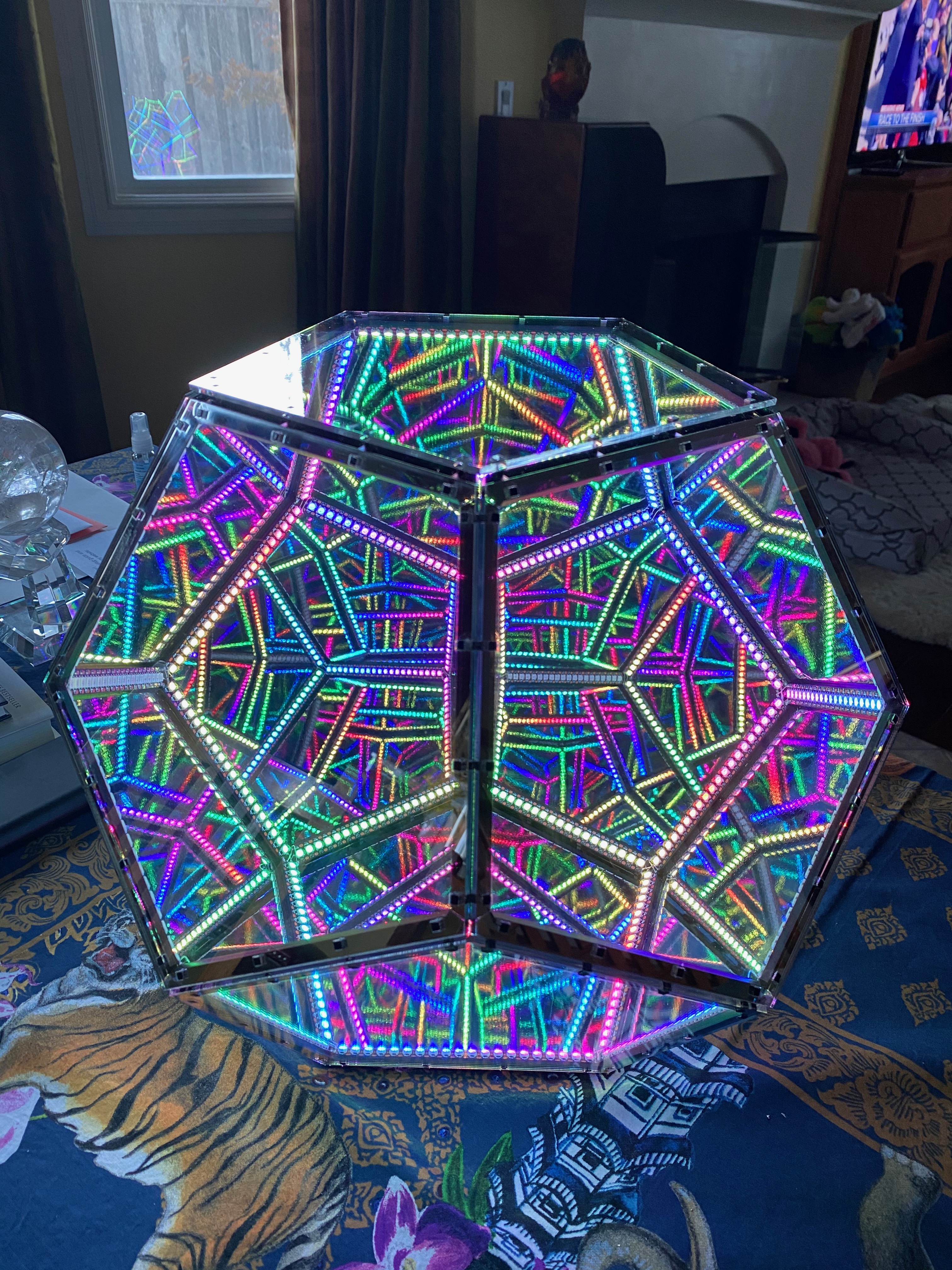
I’m new to Pixelblaze and this forum. I just built an infinity dodecahedron (6" edges with 20 pixels each edge) and fired up my first V2 yesterday and WOW! I like to get way over my head and was wondering if anyone has attempted 3D mapping one of these bad boys?
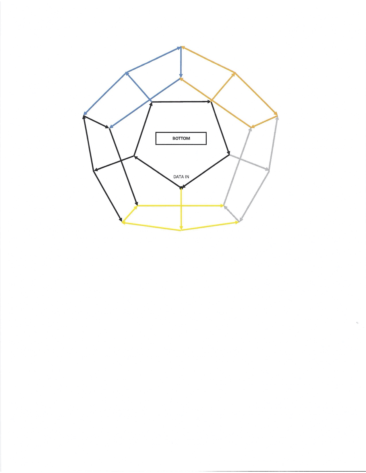
I attached a pic of the build for reference and have a strip map diagram as we (but could only load 1 image). Warning…I know “zero” about coding but am an eager/quick leaner and would appreciate any advice (other than "go back to school and study computer science).
Nice… So first step, document the strip order, label each face from top down to bottom (1-12, or A-L, etc), and list the edge order as the two faces (so AB, AC, AD, AE, AF, perhaps…)
The problem isn’t the math (which is pretty simple to calculate, as 20 points between each vertex), but the strip order to use.
I actually was thinking about a polyhedral mapper (I have a Rhombic Triacontahedron I want to map face centers for, one led per face… the problems are all similar, and I’ll just write a fairly generic mapper I think… Likely each polyhedron as a array of vertex/edges/faces…)
So here’s some helping for the labeling and the math we’ll do:
Use the “net map” to label A-L, and then number the edges in order, and post a photo of that, so we know the right order (we actually care about the edge from vertex to vertex but that’ll be clear)
Then the math of a dododeca is described in the Cartesian Coordinates section, and basically since the mapper will reorganize everything into a 0…1 format, we can do the -1,-1,-1 (etc) format and PB will magically turn that into the right values for itself. So we’ll just pick each of the 30 edges, and figure out 20 spots equally in between it’s two ends (which the math is known for), and bingo, we’ll have all 30x20 (or 600 pixels) mapped, but as I said, order matters first.
I’ll happily write up the mapper (since I’ll make it generic for other polyhedral in same way).
Wow…thanks so much and I’ll start working on that. I’ve attached the mapping of my strips for reference. I only have 1 data input and then I fork up at each of the 5 vertices with 5 dead ends which fork from the equator (if that makes sense). Thanks again and I really appreciate the help!!!
Did you design it yourself? Please let us know if you are going to post “the making of” as I’m sure I’m not the only one that would love to know how you did it.
Yes, I did make it and below is the parts list and the build sequence.
PARTS LIST:
Panels: 1/8" acrylic 2-way mirror (6 12x20 sheets from Tap Plastic “TP”)
LED Holders/Connectors: 1/8" acrylic black (1 x 12/x0 sheet from TP)
LEDs Strips: 2812B 144 pixels (5x1 meter rolls from Alitove)
Glue: Acrylic Cement (fast setting applied with bottle/syringe from TP)
Connector Wire: 22 AWG solid tinned-coper bus bar wire (Jameco)
*LED Controller: Pixelblaze V2+
BUILD SEQUENCE:
Glue LED connectors to LED Holders - make sure connectors are as vertical (90 degrees to holder) as possible to avoid fit problems with the panels.
Place Strips of 20 LED’s on each of the LED Holders (lightly sand them for better adherence) and tin connectors.
Trim all LED Strip edges so they don’t extend over LED holders and cause electrical shorts with other strips in close contact. You can trim dead end Strips shorter just to avoid any contract - I didn’t do that but would do that in the future.
Optional: I cut about 8 non-mirror acrylic panels to use as temporary Panels as I soldered the LEDs to avoid damaging the mirrors when soldering. I’m glad I did.
Insert (but don’t glue) LEDs into Panels, cut wire to exact sizes and use to connect + / - / D. Helps to use a tweezer to hold the wire in place while soldering.
Strip Pattern (see in separate thread): Looking down on the bottom panel, I ran a clockwise loop connecting the 5 Strips (100 pixels total). I then ran the following 5 upward paths at each of the 5 joints: Up, Up Right & Up Left (Up Left dead ended), Up, Up Right. This allowed no back-tracking or need for any wires other than the main wire input.
I moved around the 8 non-mirror Panels as needed (use painters tape to secure panels to each other) to ensure the LED Holders were properly positioned when soldering. It’s a bit delicate so be careful when removing and attaching and soldering as to not stress the LED strips. Arc the connector wires upward where you have to cross wire paths when connecting 1 Strip to 2 Strips (9 intersections require this).
After all Strips are soldered and tested, with the 8 non-mirror Panels still attached, Start attaching the mirror Panels one-by-one and removing the temporary Panels. This is delicate work as sometimes the square pegs don’t fit perfectly into the square holes…need to be patient and carefully maneuver / wiggle / swear at them, etc. One mirror Panel has a small hole which I use to connect my first Ptrip to my +/-/D wire input. You’ll see this on one of the Panels in AI file. Be sure to delete that hole when cutting the other 11 Panels
I didn’t glue the bottom and top mirror Panels as those will be access Panels for future maintenance.
With the 10 mirror Panels in place, time to glue the Panels to the inserted LED Connector squares being careful not to get glue spill or splash. Orient the dodecahedron so the Panel you are gluing is on top. Keep a napkin with you to catch any syringe drips. Gently squeeze the glue bottle to bleed air. With the syringe tip sideways touching the center of the black LED Connector square, let 1 (and only 1) drop of glue seep between the LED Connector squares and the Panel square holes. Do not wipe any glue and just let it dry if you get some over-run onto the panel. This takes practice and patience to avoid over-spill so you may want to practice on spare pieces. You’ll be happy with the results if you practice…let dry for 24 hours.
Clean all of the mirrors, connect to power and an LED Controller and watch the magic happen!
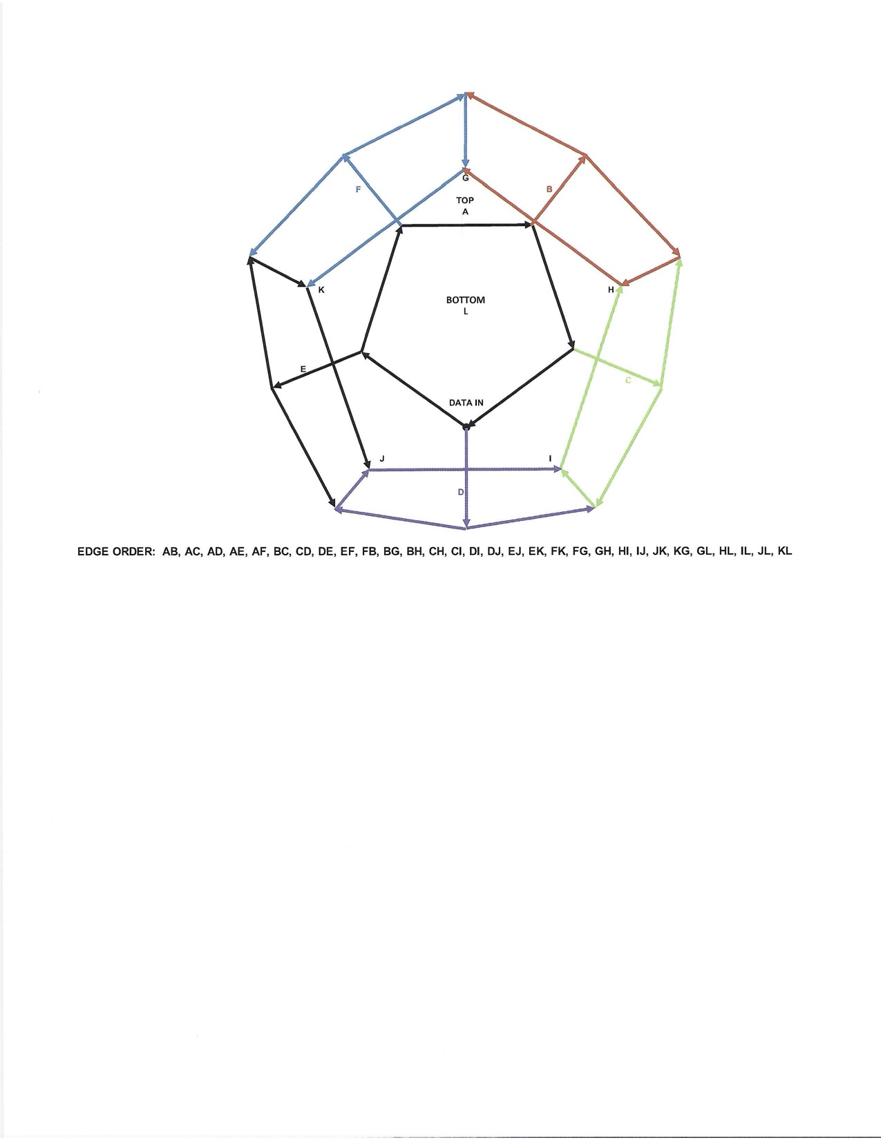
Here is the pic with the Face’s labled (A thru L) and the Edge Orders at the bottom. Each color line represent the strip orders with the data in a the bottom at the vertex of Faces L,I & J.
Your data line goes Around A, and
Then goes to BC… You have “jumpers” (wire not LEDs) not Ys anywhere, right?
Do you mean you actually joined 5 100 pixel strands all bound to same data? That’s fine, but its not 500 addressables then, it’s 100, each line will mirror.
Oh no, I think in a reread, you actually did this:
20 pixels, Y into 20pixels*2, Y again, Y again, Y again, and now you have those splits running down, yes, and another split as needed.
That’s actually worse than 5 lines of 100, its
Actually, 1-20
21-40 is 2 pixels (60 total)
41-60 is 3 pixels (120 total)
61-80 is 4 pixels (200 total)
And I suspect if you branched again, it gets worse…
Really (and incomplete) complicated map, and many pixels all linked as one pixel.
I probably didn’t explain that right. Yes, 1 data line in at the bottom that runs all edges of L (bottom).
Then I fork up at each intersection and each of those runs are mirrors of each other that go Up, Fork Up Right and Up Left with Up Left a dead end, Up and Up Left.
There is no back tracking and wires just at the joints.
So even if we find the 200 pixel path, started from wherever the data line is (A or L?) ?
It’s actually not “mirrored”, because each fork
Even if we can still map the biggest, it won’t line up with the others…
You’d be better not mapping it in 3d. Symmetries are all broken.
Use the 20 pixels as your pattern size… Everything will look best with 1d that size, repeating… It’ll mirror correctly everywhere.
You could modify any 1d pattern by setting pixelcount to 200, but limiting the pattern by replacing any pixelcount using code with “20” and then when rendering, you’d render all 200, but always calculate 21 as 1, 22 as 2 (etc), 41 as 1
To be clear, one run of 500, done in series is the only truly addressable that will give you a full grid that ever looks right. Doing 5 parallel lines, there isn’t a mirror design that can give you symmetry unless you jumped even worse (the exercise of how to show no smaller set of paths can be all symmetrical is left to the reader, as they say, but think about the fact: number of odd vertexes, aka the same thing discussed in video)
Hmmmm…I get it. That means a lot of backtracking which means I need to make a design change to accommodate wire channels which can be done. I like the challenge!!!
I am finishing up an infinity cube and luckily I considered the wiring order very early on and my wife is a math major so she could help. I still had to make some back channels for wires on one face. My aim/passion is to make all the Platonic Solids
Really nice work JerryB.